Microfabrication of Microfluidic Chips: Materials and Methods
Microfluidic chips are created using various methods (photolithography, molding, etching, embossing, 3D printing) to design micrometric structures such as channels, chambers and wells. The main materials for chip production are inorganic materials (glass, silicon, ceramic, etc), polymers (COC, PMMA, PDMS), or organic materials (generally paper).
The material dictates chip properties. It is essential to consider the end application while choosing or producing a chip. Most of the information to follow is excerpted from the Springer Handbook of Nanotechnology (Microfluidic Devices and Their Applications) written by Aryasomayajula et al.[1], and the paper “Materials for Microfluidic Chip Fabrication” by Ren et al [2].
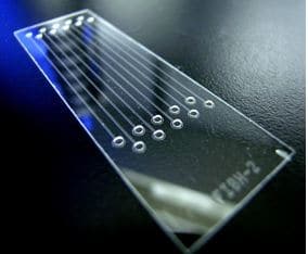
Silicon or glass microfluidic chips
Inorganic materials were the first to be used in the microfabrication of microfluidic chips, and were previously used in applications with microchannels such as glass or quartz capillaries for gas chromatography and capillary electrophoresis (CE). With the introduction of the MEMS technology, the first-generation of microfluidic chips were prepared in silicon or glass and processed with standard photolithography.
Glass is an optically transparent insulator, while silicon is opaque. Glass and silicon are highly rigid materials, have high stability at high temperatures and are highly resistant to organic solvents. Moreover, as glass/silicon chips are usually produced via photolithography, they can reach sub micrometer channel dimensions with high reproducibility. Compared to standard CE, on-chip CE is lower in cost, easier to parallel, and offers valve-free injection (utilizing the electroosmotic flow), which can separate analytes within seconds. Because of the high thermostability and solvent compatibility, on-chip reactions and droplet formation are also well-suited applications with silicon/glass.
Significant problems with using these materials for the microfabrication of microchips is high cost and the use of dangerous chemicals, which requires well-trained lab technicians at expensive facilities. These chips are also not suited for low/medium scale production and are not permeable to gas when in glass. Though they are compatible with biological samples, they are not suitable for cell culture.
Finally, high rigidity makes these materials fragile, and additional care is required when manipulating them.
These limitations led to the development of other chip materials that can be easily fabricated and are compatible with broader biological applications.
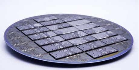
Production Methods for Silicon Microfluidic Chips: Photolithograpy
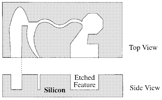
Several methods have been developed for the microfabrication of microfluidic chips with silicon, including bulk micro-machining, surface micromachining and buried channel methods.
- Bulk micro-machining is a photolithography method to pattern desired micro features on a substrate (here, silicon)3. Two etching methods exist: dry etching and wet etching. Dry etching refers to the removal of material by exposing it to a bombardment of ions (usually a plasma of reactive gases) that dislodge portions of the material from the exposed surface. In wet etching, the wafer is typically immersed in a bath of etchant. For instance, buffered hydrofluoric acid (BHF) is used commonly to etch silicon dioxide over a silicon substrate. After etching, another substrate such as glass or silicon is bonded to the patterned piece to form enclosed channels, chambers and other features.
- Surface micromachining for the fabrication of microfluidic chips builds microstructures by deposition and etching structural layers over a substrate4. It is grounded in the use of photolithography to define patterns that are selectively subjected to chemical processing steps that either modify the properties of the silicon substrate or define the geometries of overlying thin films deposited on the substrate. SiO2 and Si3N4 are typically used as “sacrificial” materials (removed material) while polysilicon (poly-Si) is used to form the structural layer1.
- The buried channel technique is a bonding-free approach. The microstructures are constructed by trench etching, coating of the sidewalls of the trench, removal of the coating at the bottom of the trench, and isotopically etching of the channel into the bulk of the silicon substrate5. Additional information on the production of microfluidic chips with this technique can be found in the paper written by de Boer et al.5 The structures can be sealed by deposition of a suitable layer that closes the trench.
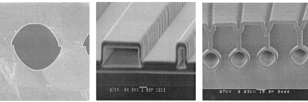
Methods of fabricating glass microchannels are not as diverse and advanced as silicon, and are mostly fabricated with mechanical, wet or dry etching approaches.
Silicon and glass: the bottom line
- Silicon and glass were the first materials used in microfluidics
- Inspired from MEMS technology, silicon can easily reach sub micrometer channel resolution
- They are highly rigid materials, have high stability at high temperature and are highly resistant to organic solvents
- The high production costs motivated the development of chips using other materials
Fabrication of Polymers Microfluidic Chips
Polymer-based microfluidic chips were introduced several years after silicon and glass chips. The wide variety of polymers grants great flexibility in choosing a suitable material with specific properties. In the microfabrication of microfluidic chips, polymers offer an attractive alternative to glass and silicon as they are easy to access, usually less expensive, and have suitable physical properties.
Many polymers can be used to build chips, such as polystyrene (PS) polycarbonate (PC), polyvinyl chloride (PVC), cyclic olefin copolymer (COC), polymethylmethacrylate (PMMA) or polydimethylsiloxane (PDMS). Polymers can be classified into three different groups: elastomers, thermoplastics, and thermosets.
Elastomers microfluidic chip
Elastomers are amorphous polymers maintained above their glass transition temperature so that considerable molecular reconformation-without breaking of covalent bonds- is feasible. At ambient temperature, such materials are relatively compliant and deformable: they can stretch or compress when external force is exerted and return to the original shape when the external force is withdrawn.
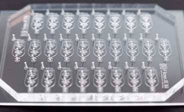
Though PDMS is useful for easy and fast prototyping, soft lithography is not well suited for mass production. In the microfabrication of microfluidic chips, reproducibility is a challenge, and it is time-consuming to make a large number of devices. PDMS is also hydrophobic.
As a consequence, hydrophobic analytes can adsorb onto the PDMS surface, potentially interfering with analysis. Surface treatments can be performed to mitigate issues, but can also be time-consuming, and the treatment can lose its efficiency over time. They are not suitable for high-pressure operations as higher pressures alter channel geometry, making the treatment prone to leaking at elevated pressure.
Soft lithography for the production of PDMS microfluidic chips
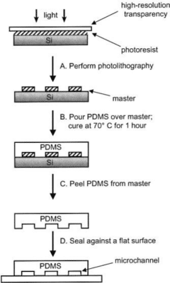
Figure 3: (A) The mold master is produced by patterning photosensitive resin exposed through a photomask (high resolution transparency) that contains the design of the microchannel. (B) Liquid PDMS is poured over the master and cured for 1 h at 70°C. (C) The PDMS replica is peeled from the master, and (D) the replica is sealed to a flat surface to enclose the channels. The overall process takes about 24 h6.
PDMS is the material of choice for fast production of microfluidic chips, and PDMS chips are thus commonly used in laboratories, especially in the academic field.
The most popular fabrication method for producing PDMS chips is soft lithography. In this method, liquid PDMS is mixed with a curing agent to crosslink the polymer. The amount of curing agent used defines the hardness of the final product. The whole solution is subsequently cast over a master (typically silicon-based) mold (figure 2). The master is placed in an oven at around 60°C for 1 h to 4 h to allow crosslinking.
Once cured, the PDMS is easily peeled off from the master mold. At this point, open channels are obtained, and the PDMS needs to be bonded to another surface to form enclosed channels.
It can be bonded to several materials, such as glass or back to PDMS. This is done by performing a plasma treatment on the surfaces to be bonded (most common method), or mechanical or chemical bonding.
Thermoplastics polymers
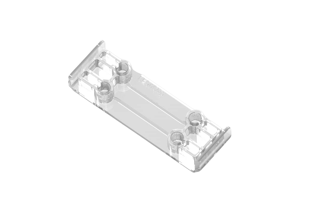
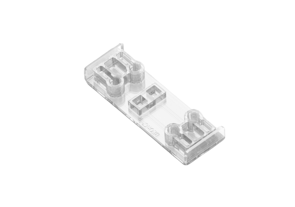
Thermoplastics are widely used materials in the microfabrication of microfluidic chips as they are transparent materials that allow microscopic analysis. Thermoplastics are highly crosslinked polymers that can retain their shape after cooling. Thermoplastics are usually fabricated by thermomolding that allows the production of thousands of replicas at high rate and low cost, which is excellent for commercial production. Using them, it is possible to reach sub micrometer channel dimensions.
Depending on their application, the surface of thermoplastics can be modified by coating or surface grafting. Covalently modified surfaces are generally more stable for thermoplastics than PDMS. They can be easily integrated with electrodes for flexible circuits.
Poly-methyl methacrylate (PMMA) microfluidic chip
PMMA is a low-cost polymer with superior mechanical strength, electrical insulation, and transparency compared to PDMS. PMMA shows high biocompatibility and is a suitable candidate for biomedical and disposable point-of-care devices. The microfabrication of PMMA microfluidic chips is typically done using a hot embossing technique, but mass production of PMMA devices can be achieved with an injection molding method that facilitates shorter fabrication cycle times1.
Most production methods for thermoplastics are excellent for commercial production, but not economical for prototype development. As thermoplastics are barely permeable to gas, their sealed microchannels and microchambers are unsuitable for long-term cell study or cell culture.
Thermoset polyester (TPE) microfluidic chip
A thermoset is a polymer that irreversibly becomes rigid when heated. Initially, the polymer is a liquid or soft solid. When heated or radiated, the thermosetting molecules cross-link to form a rigid network that cannot soften before decomposition. These materials are normally stable (even at high temperatures), resistant to most solvents, and optically transparent.
Microfluidic chips can be entirely fabricated in thermosetsusing injection molding methods. Thermosets usually have a higher rigidity compared to elastomers and thermoplastics. However, due to their high cost, the microfabrication of microfluidic chips with thermosets remains limited.
Why Use Polymers?:
- Introduced several years after silicon and glass
- A wide variety of polymers exist, granting great flexibility in choosing a suitable material with specific properties
- PDMS is one of the most commonly used material for chip fabrication
- Thermoplastics, such as PMMA, are favored for microfluidic chip mass production
Paper Microfluidic Chips Fabrication
Paper is a highly porous matrix made of cellulose, excellent in wicking liquids. When certain areas of a paper are modified hydrophobically, an aqueous solution applied to the paper will be precisely guided through the hydrophilic region by the capillary effect.
Elastomers
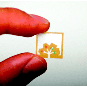
The microfabrication of paper-based microfluidic chips is relatively simple and flexible, allowing to balance between channel resolution and cost. The utilization of paper as chip material leads to several advantages. The microchannel can act as a passive pump dispenser (without the need of power or external components); paper is one of the cheapest materials for microfluidics, and fabrication by printing is convenient and low-cost. Paper-based microfluidic devices are promising in portable and low-cost analysis, especially for bioassay-based personalized medical care.
Working with such materials brings several challenges. Channel dimensions are wide (not lower than 200 µm, while 20 μm wide channels are common for other materials) and some liquids with low surface tension may not be well confined into hydrophobic channels. It is also not suited for operating with an external pump or dispenser. As a result, few microfluidic applications have been demonstrated on paper chips.
Production of microfluidic chips with paper methods
Many methods exist for the microfabrication of microfluidic chips with paper, including wax printing, inkjet printing, but also flexographic printing, screen-printing, wax screen-printing, paper cutting, and even photolithography.
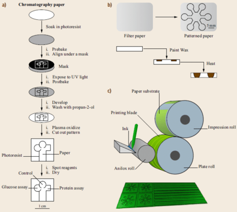
Most of these techniques, except paper cutting, rely on patterning paper with hydrophobic materials to define the microchannel boundaries and confine the fluid flow. In the wax printing process, the filter paper is patterned with microchannels using a wax pen and a template ruler (figure 3 b). The patterned paper is subsequently placed in an oven, causing the wax to melt and penetrate the paper, forming hydrophobic walls and causing liquid flows inside the edges of the wax wall.Because of the need for mass abrication of microfluidic chips, a method based on flexographic printing has been developed7.
A substrate paper made of polystyrene is fixed to an impression roll. The ink is applied into the reservoir by a pipette (figure 3c). The ink transfers onto an anilox roll covered by thousands of small cells. When the printing process starts, the anilox roll accelerates to the printing speed and rotates to distribute the ink. Then, the plate and impression roll rotate through one revolution to transfer the ink onto the paper substrate.
Why use paper for a microfluidic chip?
- Development of paper-based microfluidic devices began in the early 21st century
- It meets a need for inexpensive and portable medical diagnostic systems
- Channel dimensions are wide compared to other materials (not lower than ~ 200 µm)
- Not suited for operating with external pumps
Integration of hydrogels in microfluidic chips
Hydrogels are widely used in the microfabrication of microfluidic chips. Hydrogels are 3D networks of hydrophilic crosslinked polymer chains that span in aqueous medium. Heating, exposure to UV light and using chemical chelators are common methods to have the hydrogel chains crosslinked to form desired networks. They are highly absorbent (they can contain over 90% water) natural/synthetic polymeric networks and highly porous, allowing for molecules or particles to diffuse through.
Hydrogels are the perfect material for encapsulating cells because of their hydrophilic nature, high permeability, transparency, and their biocompatibility. They have been used in many applications such as cell-to-cell interaction, drug delivery, artificial tissue constructs, and regenerative medicine1. In recent years, with the fabrication of microfluidic chips, a variety of microfluidic 3D cell culture platforms have been developed for recreating complex and well-controlled 3D microenvironments that mimic the biological niche.
In particular, culturing cells in hydrogels has shown to be useful in helping cells retain their native tissue-specific functions by mimicking the in vivo 3D tissue environment. The combination of 3D-hydrogel cell cultures with microfluidics offers several advantages including appropriate microscale dimensions that are comparable to in vivo microstructures, the establishment of chemical gradients to create dynamic 3D microenvironments, and creation of reproducible medium-matrix biointerfaces8.
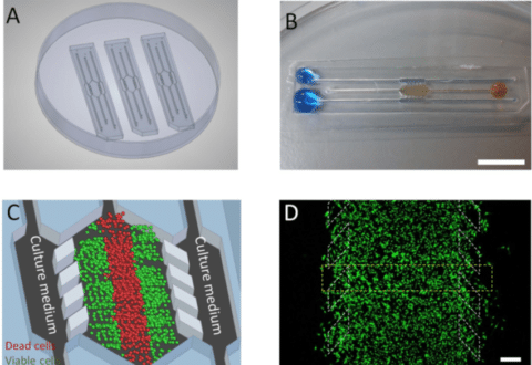
Figure 5 : (A) 3 microdevices in a Petri dish containing a central culture chamber (detailed in C) and 6 channels. (B) One microdevice is filled with (yellowish) collagen hydrogel flowing to the microchamber from the right middle channel and blue-colored water perfused through the two lateral microchannels. (C) Culture medium perfused through the lateral microchannels. (D) Cellular monitoring with fluorescent dye in the microdevice9.
Production of hydrogels microfluidic chips
Several methods exist for the integration of hydrogels in microfluidics, including a soft lithography-based approach with sacrificial or reusable templates, photopolymerization, and local integration10. Over the past decade, hydrogels, such as agarose, Matrigel, polyethylene glycol diacrylate (PEG-DA) alginate, and chitosan, have been frequently used in the microfabrication of microfluidic chips.
Gels like agarose are commercially available and relatively inexpensive, thus easy to obtain. Moreover, gels are malleable and available in various designs and size calibrations, allowing for quantitative fabrication.
- Soft lithography for gel micro-fabrication is similar to the soft lithographic methods explained in the polymers section. As most gel materials can maintain a liquid state before they solidify into a gel state, liquid gel can be poured into a designed template and replicate the structure from the mold. The solidified gel can easily be peeled off from a photoresist or PDMS molds. Using this method, hydrogels can be used in the production of microfluidic chips or cell confinement structures. The traditional soft lithography microfluidic method can easily fabricate a device with two-dimensional complexity or quasi-2D layered structure upon exact placement of each element. For applications demanding 3D architectures but not accurate channel size, a 3D and degradable template coated with hydrogel can be produced. The template is subsequently sacrificed to generate microfluidic structures in the bulk materials. More information can be found in the paper written by Zhang et al.10
- In the local integration method, the creation of gel structures is performed in a microfluidic device. Because of the laminar nature of flow in microfluidic systems, various gels can be co-introduced in a microchannel, and these flows form a laminated structure (figure 4b). In this method, for the microfabrication of microfluidic chips, the microfluidic channel is thus divided into multiple layers separated by microslabs of hydrogels. A solidification process is finally performed. Many studies recently used flow-solidification based gel integration methods to produce hydrogels.
- In the photopolymerization technique, for integrating microstructures into the microsystem, a UV light is employed to construct gel structures with high spatial resolution. Uniform exposure, printing with a mask and directed writing are the three common types of photopolymerization used to form the structured gel components in a device. High spatial resolution and high aspect ratio features are achievable using this method1.
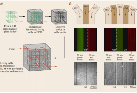
Figure 6: 3-D vascular network that was fabricated using a 3-D printed sacrificial template followed by encapsulation in ECM and dissolving in lattice cell media. (b) Formation of microslabs of hydrogel by colaminar flows in a microchannel 1
About Hydrogels
- Hydrogels, such as agarose, matrigel, polyethylene glycol diacrylate (PEG-DA), alginate, and chitosan, have been used in the fabrication of microfluidic chips, mostly for biological studies
- Recently, a variety of microfluidic 3D cell culture platforms in hydrogels have been developed
- They allow experimenters to recreate complex and well-controlled 3D microenvironments that mimic the biological niche
- They are easy to obtain and can produce quantitative fabrication
Conclusion
Since its introduction, microfluidics continues to advance with technology and expand the fields of application. In terms of chip materials and functions, while glass and silicon have important uses, polymeric materials have become the material of choice for the microfabrication of microfluidic chips. Hydrogel and papers are recently-used materials in microfluidics for specific applications.
Two tables from the paper of Ren and al. summarize various properties of each material and their typical applications. This study provides an overview of material properties and applications. A detailed study of materials should be performed to ensure proper function for a specific applications.
Table 1: Summary of properties as a function of the material2.

Table 2: Summary of application as a function of the material2.

How to choose a microfluidic chip
If you wonder how to choose a microfluidic chip, here are some key information to consider:
- Transparent materials are favored to enable optical observation/analysis.
- Materials with a low autofluorescence are crucial for optimal detection by fluorescence and laser induced fluorescence techniques.
- Materials must be biocompatible for life science applications.
- Most of the chips need surface treatment to adapt their surface properties to the application and to limit non-specific adsorption.
Expertises & Resources
-
Microfluidic Application Notes Automating Neuronal Cell Immunofluorescence in Microfluidic Chips Read more
-
Interviews & Testimonials Panel Discussion & Interviews – Microfluidics & Organ-On-Chips Read more
-
Microfluidics White Papers Microfluidic white paper – A review of Organ on Chip Technology Read more
-
Expert Reviews: Basics of Microfluidics How to choose a microfluidic chip Read more
-
Microfluidic Application Notes Peristaltic Pump vs Pressure-Based Microfluidic Flow Control for Organ on Chip applications Read more
-
Expert Reviews: Basics of Microfluidics Mastering Microfluidic Chips: An In-Depth Definition Read more
-
Expert Reviews: Basics of Microfluidics Application of microfluidic chip technology Read more
Related Products
References
- Aditya Aryasomayajula, Pouriya Bayat, Pouya Rezai, P. R. S. Microfluidic Devices and Their Applications. Springer vol. 50 (2017).
- Ren, K., Zhou, J. & Wu, H. Materials for microfluidic chip fabrication. Acc. Chem. Res. 46, 2396–2406 (2013).
- Kovacs, G. T. A., Maluf, N. I. & Petersen, K. E. Bulk micromachining of silicon. Proc. IEEE 86, 1536–1551 (1998).
- Bhat, K. N. Micromachining for microelectromechanical systems. Def. Sci. J. 48, 5–19 (1998).
- De Boer, M. J. et al. Micromachining of buried micro channels in silicon. J. Microelectromechanical Syst. 9, 94–103 (2000).
- McDonald, J. C. & Whitesides, G. M. Poly(dimethylsiloxane) as a material for fabricating microfluidic devices. Acc. Chem. Res. 35, 491–499 (2002).
- Olkkonen, J., Lehtinen, K. & Erho, T. Flexographically printed fluidic structures in paper. Anal. Chem. 82, 10246–10250 (2010).
- M and Badre, D. Ö. L. N. Microfluidic 3D cell culture: potential application for tissue- based bioassays. Bioanalysis 23, 1–7 (2012).
- Ayuso, J. M. et al. Development and characterization of a microfluidic model of the tumour microenvironment. Sci. Rep. 6, 1–16 (2016).
- Zhang, X., Li, L. & Luo, C. Gel integration for microfluidic applications. Lab Chip 16, 1757–1776 (2016).
